In four talks over two days, senior NVIDIA engineers will describe innovations in accelerated computing for modern data centers and systems at the edge of the network.
Speaking at a virtual Hot Chips event, an annual gathering of processor and system architects, they’ll disclose performance numbers and other technical details for NVIDIA’s first server CPU, the Hopper GPU, the latest version of the NVSwitch interconnect chip and the NVIDIA Jetson Orin system on module (SoM).
The presentations provide fresh insights on how the NVIDIA platform will hit new levels of performance, efficiency, scale and security.
Specifically, the talks demonstrate a design philosophy of innovating across the full stack of chips, systems and software where GPUs, CPUs and DPUs act as peer processors. Together they create a platform that’s already running AI, data analytics and high performance computing jobs inside cloud service providers, supercomputing centers, corporate data centers and autonomous systems.
Inside NVIDIA’s First Server CPU
Data centers require flexible clusters of CPUs, GPUs and other accelerators sharing massive pools of memory to deliver the energy-efficient performance today’s workloads demand.
To meet that need, Jonathon Evans, a distinguished engineer and 15-year veteran at NVIDIA, will describe the NVIDIA NVLink-C2C. It connects CPUs and GPUs at 900 gigabytes per second with 5x the energy efficiency of the existing PCIe Gen 5 standard, thanks to data transfers that consume just 1.3 picojoules per bit.
NVLink-C2C connects two CPU chips to create the NVIDIA Grace CPU with 144 Arm Neoverse cores. It’s a processor built to solve the world’s largest computing problems.
For maximum efficiency, the Grace CPU uses LPDDR5X memory. It enables a terabyte per second of memory bandwidth while keeping power consumption for the entire complex to 500 watts.
One Link, Many Uses
NVLink-C2C also links Grace CPU and Hopper GPU chips as memory-sharing peers in the NVIDIA Grace Hopper Superchip, delivering maximum acceleration for performance-hungry jobs such as AI training.
Anyone can build custom chiplets using NVLink-C2C to coherently connect to NVIDIA GPUs, CPUs, DPUs and SoCs, expanding this new class of integrated products. The interconnect will support AMBA CHI and CXL protocols used by Arm and x86 processors, respectively.

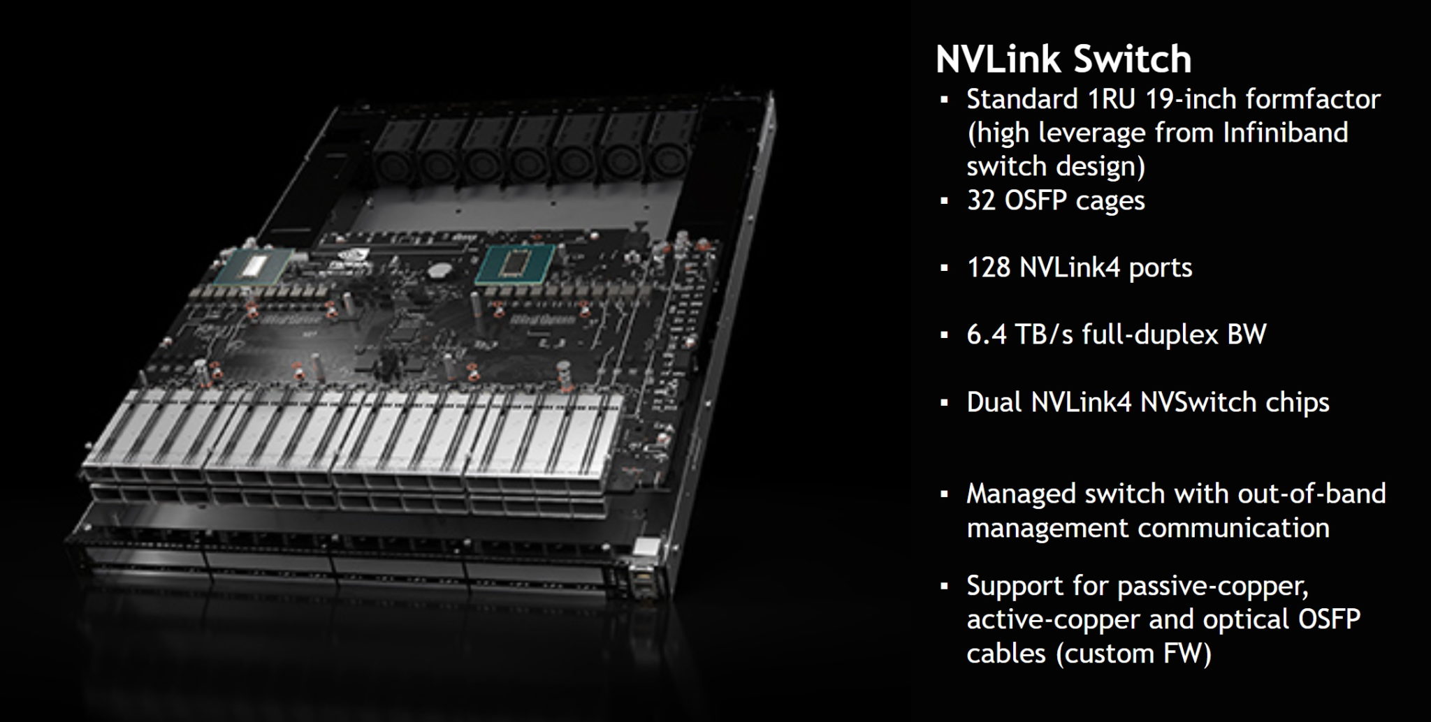
To scale at the system level, the new NVIDIA NVSwitch connects multiple servers into one AI supercomputer. It uses NVLink, interconnects running at 900 gigabytes per second, more than 7x the bandwidth of PCIe Gen 5.
NVSwitch lets users link 32 NVIDIA DGX H100 systems into an AI supercomputer that delivers an exaflop of peak AI performance.
Alexander Ishii and Ryan Wells, both veteran NVIDIA engineers, will describe how the switch lets users build systems with up to 256 GPUs to tackle demanding workloads like training AI models that have more than 1 trillion parameters.
The switch includes engines that speed data transfers using the NVIDIA Scalable Hierarchical Aggregation Reduction Protocol. SHARP is an in-network computing capability that debuted on NVIDIA Quantum InfiniBand networks. It can double data throughput on communications-intensive AI applications.
Jack Choquette, a senior distinguished engineer with 14 years at the company, will provide a detailed tour of the NVIDIA H100 Tensor Core GPU, aka Hopper.
In addition to using the new interconnects to scale to new heights, it packs many advanced features that boost the accelerator’s performance, efficiency and security.
Hopper’s new Transformer Engine and upgraded Tensor Cores deliver a 30x speedup compared to the prior generation on AI inference with the world’s largest neural network models. And it employs the world’s first HBM3 memory system to deliver a whopping 3 terabytes of memory bandwidth, NVIDIA’s biggest generational increase ever.
Among other new features:
- Hopper adds virtualization support for multi-tenant, multi-user configurations.
- New DPX instructions speed recurring loops for select mapping, DNA and protein-analysis applications.
- Hopper packs support for enhanced security with confidential computing.
Choquette, one of the lead chip designers on the Nintendo64 console early in his career, will also describe parallel computing techniques underlying some of Hopper’s advances.
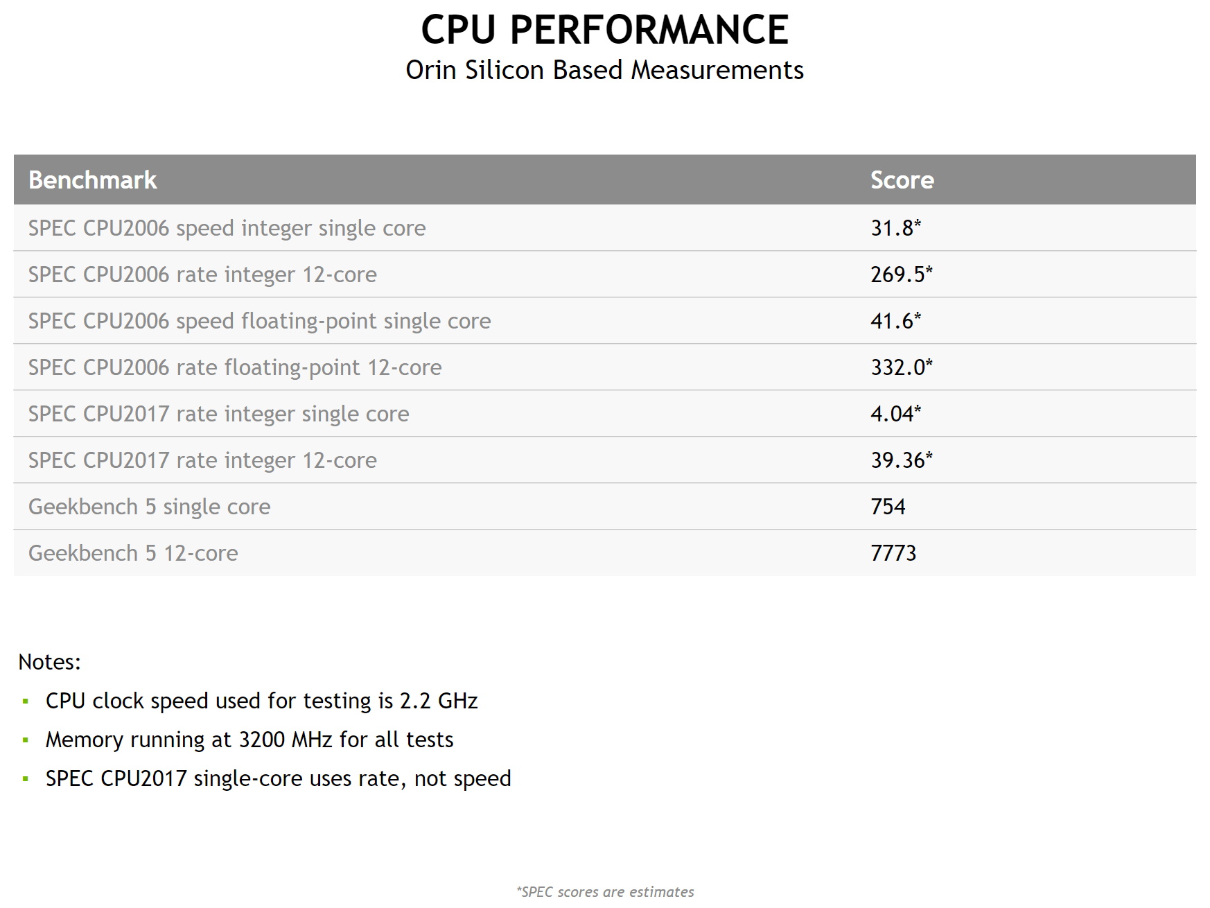
Michael Ditty, chief architect for Orin and a 17-year tenure at the company, will provide new performance specs for NVIDIA Jetson AGX Orin, an engine for edge AI, robotics and advanced autonomous machines.
It integrates 12 Arm Cortex-A78 cores and an NVIDIA Ampere architecture GPU to deliver up to 275 trillion operations per second on AI inference jobs. That’s up to 8x greater performance at 2.3x higher energy efficiency than the prior generation.
The latest production module packs up to 32 gigabytes of memory and is part of a compatible family that scales down to pocket-sized 5W Jetson Nano developer kits.
All the new chips support the NVIDIA software stack that accelerates more than 700 applications and is used by 2.5 million developers.
Based on the CUDA programming model, it includes dozens of NVIDIA SDKs for vertical markets like automotive (DRIVE) and healthcare (Clara), as well as technologies such as recommendation systems (Merlin) and conversational AI (Riva).
The NVIDIA AI platform is available from major cloud services and system makers.
For more details, read technical blogs on Grace and NVLink written by Hot Chips speakers.