NVIDIA hardware products are feats of engineering, consisting of tens of thousands of components that work in harmony. As their complexity grows, so does the risk of component failure.
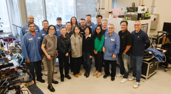
That’s why we have a dedicated failure analysis team. They’re a small, passionate crew of engineers who investigate when something goes wrong with a product.
Solving some of the toughest problems in the semiconductor industry, the team is responsible for identifying the root cause of any malfunction, whether it’s due to a design flaw, a production glitch, a reliability test failure or a foreign contaminant.
Issues can be obvious and easy to fix, or as difficult as using a telescope to find as an astronaut’s footprints on the moon. NVIDIA’s latest Hopper chips are packed with 80 billion transistors, tiny switches that control the flow of electricity. If just one of them — 10,000x smaller than the diameter of a human hair — is defective, the whole chip can fail.
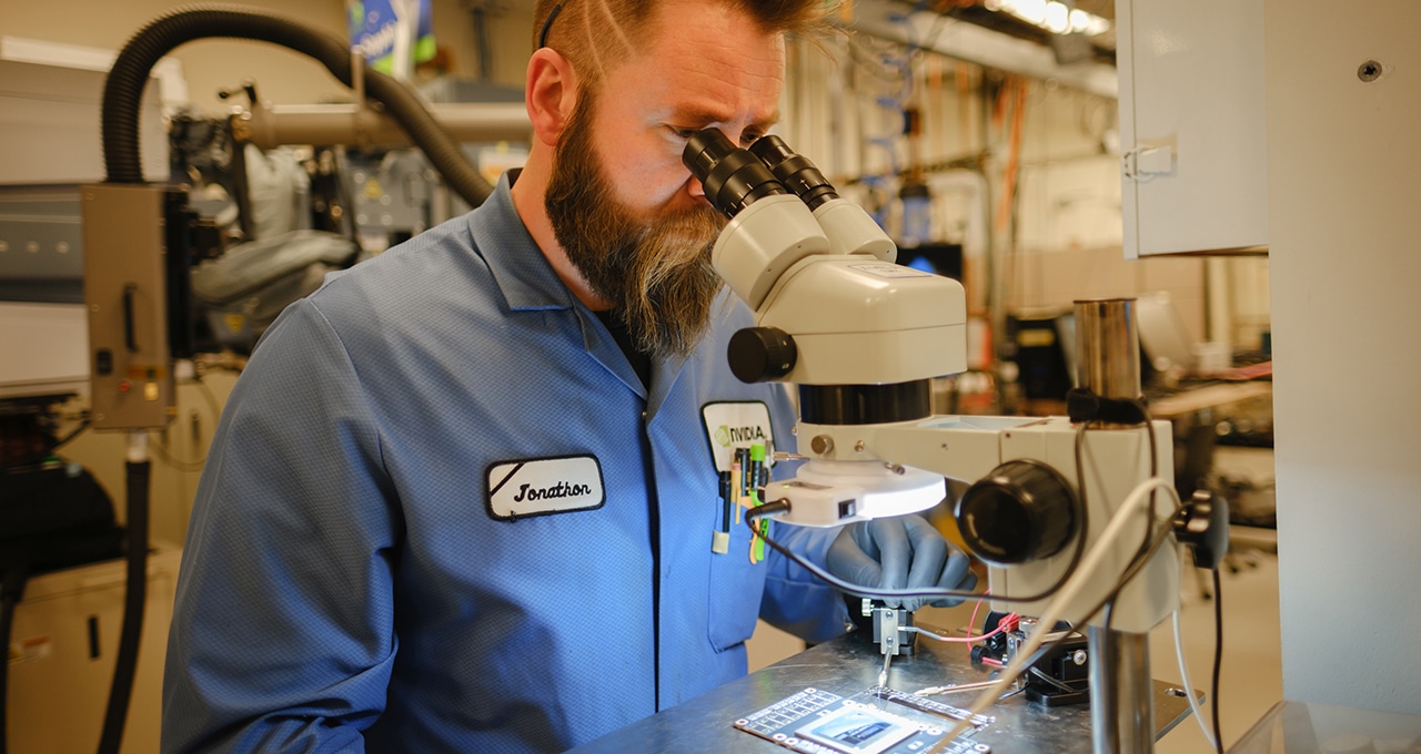
“If you think about every semiconductor company’s failure analysis lab as an NBA basketball team, NVIDIA’s group is the Harlem Globetrotters,” said Jonathon Elliott, a failure analysis engineer. “We’re doing all the trick shots that people think aren’t possible.”
A World-Class Team
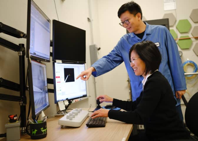
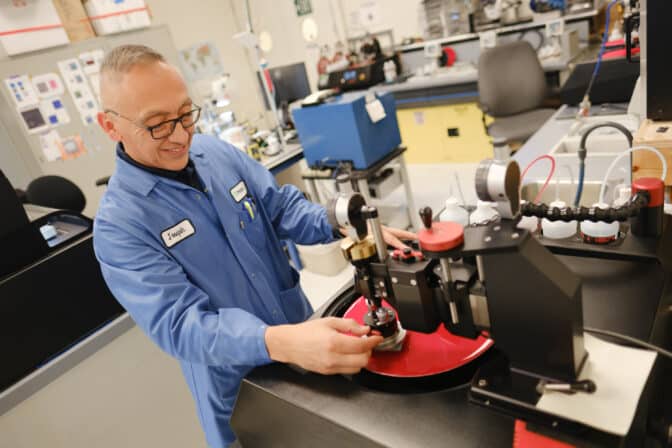
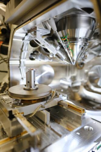
The failure analysis lab hums and hisses with the sound of highly sophisticated specialized equipment in action. The team uses complex techniques including laser voltage probing and imaging, scanning electron microscopy, pulse reflectometry, nanoprobing, thermography and X-ray imaging to identify different kinds of failures.
“NVIDIA has invested in both building a world-class lab and cultivating an exceptional team,” says Jane Li, senior manager of silicon failure analysis. “The team’s consistently amazing, innovative work propels us toward even greater success.”
“Having in-house failure analysis experts is of great value to the company,” added Joy Liao, senior manager of silicon failure analysis. “Their identification of the root cause of even a single failure can unblock a product from getting to market.”
To improve accuracy and efficiency, the team is constantly exploring new methods and developing leading-edge solutions. For example, to shorten the 12-hour turnaround time for processing 3D X-rays, they applied NVIDIA GPUs and NVIDIA CUDA and accomplished the task in just five minutes.
Achieving Excellence Through Close Collaboration
The failure analysis team collaborates with groups across NVIDIA to troubleshoot issues at every phase of the product lifecycle — from early yield ramping and silicon tapeout to reliability testing and field failures.
They work closely with the advanced technology group to analyze next-generation chips that are in development; with reliability teams who stress-test new products to find potential failure points; and with support teams to ensure that customers’ hardware is working smoothly.
“I can give the failure analysis team a board returned by a customer, and in a few days, they’ll tell me the intricate details of why and how it failed,” said Phillip Yu, senior director of customer and product quality engineering. “To be able to physically isolate and take pictures of a failed transistor when there are billions of them is real-life magic.”
Taking on Projects, Big and Small
The bustling lab churns through dozens of requests each week, from business-critical deep dives to occasional side projects for colleagues and friends.
Longtime NVIDIAN Khanh Giang, principal failure analysis engineer, recalls testing an NVIDIA GPU in December 2000 while colleagues were having a holiday party next door.
“Around 3 a.m., as I finished setting up the microprobing station and the chip went live, the entire engineering team, led by Jensen, erupted in cheers to match the party spirit in the next room,” he said, referring to NVIDIA’s founder and CEO.
In 2022, team members in Santa Clara and Hsinchu, Taiwan, collaborated to quickly troubleshoot a manufacturing issue.
“Down time is an unforgiving adversary in the production line,” said Nick Poudel, who works on electrical failure analysis. “In that critical moment, we were able to get from log analysis and software diagnosis to a successful result in just 72 hours.”
In their spare time, the team has used their water jet cutter to slice in half the cooler of an NVIDIA RTX 4090 GPU for an NVIDIA GeForce collaboration with the popular Gamers Nexus YouTube channel. They’ve also used isopropyl alcohol and an industrial oven to help fellow NVIDIANs salvage laptops from coffee spills.
Learn more about NVIDIA life, culture and careers.