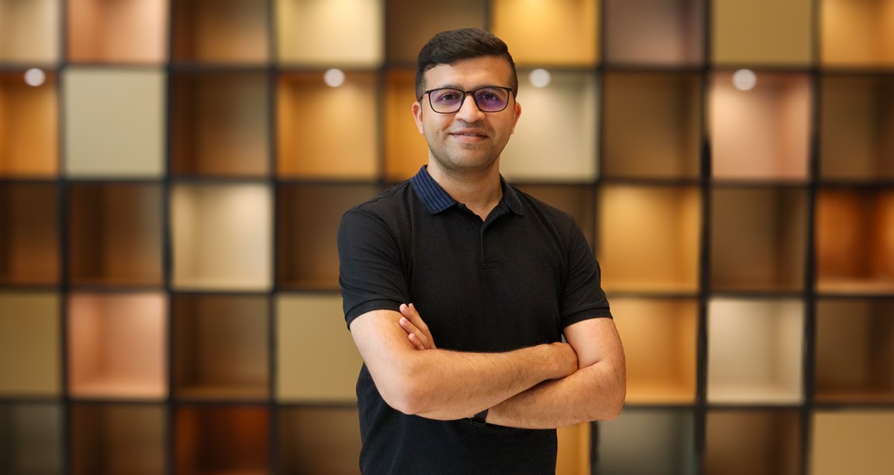
For senior application-specific integrated circuit (ASIC) engineer Tarun Patil, technology was more than a childhood curiosity — it was a calling. Today, he’s part of NVIDIA’s specialized circuit silicon correlation (CSC) team, contributing advancements in silicon debug and performance analysis methodologies.
Growing up in Shimoga, a small town in northern Karnataka, India, Patil was far from the tech hubs of the world. His father was an agriculturalist, but he had little interest in farming. Instead, Patil set his sights on engineering.
“Seeing my uncles and aunts pursue careers in tech sparked my imagination,” he said. “I knew early on that I wanted to do something in this space.”
Patil earned his bachelor’s degree in electronics and communications from the RV College of Engineering in Bangalore before moving to the U.S. to pursue a master’s degree in computer engineering at Virginia Tech.
NVIDIA was among the top companies Patil aspired to work for once he graduated. A pivotal moment came in 2019 when Patil lost his father, prompting him to reflect on his priorities.
“I enjoyed my life in the U.S., but I wanted to be closer to my family in India,” he said.

That same year, he moved back to India and joined NVIDIA, where he’s since been working on improving silicon performance analysis, as part of the CSC team. Their work plays a crucial role in the larger global circuits team by providing feedback on silicon performance versus pre-silicon design.
“It’s a cross-functional role, and we collaborate closely with teams like ASIC physical design, circuit design, memory design, design-for-test and product engineering,” Patil said. “Our feedback helps improve design accuracy, boost performance, improve test quality, fabrication process fix and significantly reduce silicon debug costs, ultimately speeding up time to market.”
One of the team’s key innovations is the first failure analysis methodology, an advanced silicon debug tool that’s been instrumental in debugging silicon for major NVIDIA projects, including the NVIDIA Ampere, NVIDIA Hopper and NVIDIA Ada Lovelace architectures.
Patil’s journey in CSC wasn’t without its challenges.
“When I joined, my background was primarily in design for test,” he said. “I had to quickly ramp up in circuit design and timing methodologies and memory design — and then figure out how to apply design-for-test principles to new areas.”

The CSC team is now focused on exploring new frontiers in silicon performance analysis for memory — an area that Patil is particularly excited about.
“There’s a lot of potential to deepen our understanding of how memory behaves in silicon compared to pre-silicon design,” he said. “This insight will help us understand what causes memory failures in silicon with better accuracy, potentially improving test quality and performance.”
Patil is grateful for the mentors and support he’s found at NVIDIA. He values the company’s flat structure and collaborative culture.
“There are no barriers here,” he said. “People are open, and the focus is on solving problems together.”
He recalls a piece of wisdom from a senior leader at NVIDIA that continues to inspire him: “Innovation happens at the boundary of multiple streams.” It’s a mindset that perfectly captures Patil’s own path, bridging disciplines and pushing boundaries to make an impact.
Follow @nvidialife on Instagram and learn more about NVIDIA life, culture and careers.


