TSMC, the world leader in semiconductor manufacturing, is moving to production with NVIDIA’s computational lithography platform, called cuLitho, to accelerate manufacturing and push the limits of physics for the next generation of advanced semiconductor chips.
A critical step in the manufacture of computer chips, computational lithography is involved in the transfer of circuitry onto silicon. It requires complex computation — involving electromagnetic physics, photochemistry, computational geometry, iterative optimization and distributed computing. A typical foundry dedicates massive data centers for this computation, and yet this step has traditionally been a bottleneck in bringing new technology nodes and computer architectures to market.
Computational lithography is also the most compute-intensive workload in the entire semiconductor design and manufacturing process. It consumes tens of billions of hours per year on CPUs in the leading-edge foundries. A typical mask set for a chip can take 30 million or more hours of CPU compute time, necessitating large data centers within semiconductor foundries. With accelerated computing, 350 NVIDIA H100 Tensor Core GPU-based systems can now replace 40,000 CPU systems, accelerating production time, while reducing costs, space and power.
NVIDIA cuLitho brings accelerated computing to the field of computational lithography. Moving cuLitho to production is enabling TSMC to accelerate the development of next-generation chip technology, just as current production processes are nearing the limits of what physics makes possible.
“Our work with NVIDIA to integrate GPU-accelerated computing in the TSMC workflow has resulted in great leaps in performance, dramatic throughput improvement, shortened cycle time and reduced power requirements,” said Dr. C.C. Wei, CEO of TSMC, at the GTC conference earlier this year.
NVIDIA has also developed algorithms to apply generative AI to enhance the value of the cuLitho platform. A new generative AI workflow has been shown to deliver an additional 2x speedup on top of the accelerated processes enabled through cuLitho.
The application of generative AI enables creation of a near-perfect inverse mask or inverse solution to account for diffraction of light involved in computational lithography. The final mask is then derived by traditional and physically rigorous methods, speeding up the overall optical proximity correction process by 2x.
The use of optical proximity correction in semiconductor lithography is now three decades old. While the field has benefited from numerous contributions over this period, rarely has it seen a transformation quite as rapid as the one provided by the twin technologies of accelerated computing and AI. These together allow for the more accurate simulation of physics and the realization of mathematical techniques that were once prohibitively resource-intensive.
This enormous speedup of computational lithography accelerates the creation of every single mask in the fab, which speeds the total cycle time for developing a new technology node. More importantly, it makes possible new calculations that were previously impractical.
For example, while inverse lithography techniques have been described in the scientific literature for two decades, an accurate realization at full chip scale has been largely precluded because the computation takes too long. With cuLitho, that’s no longer the case. Leading-edge foundries will use it to ramp up inverse and curvilinear solutions that will help create the next generation of powerful semiconductors.
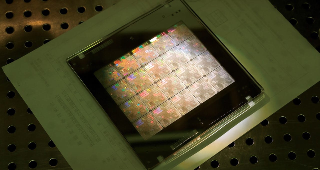
Image courtesy of TSMC.