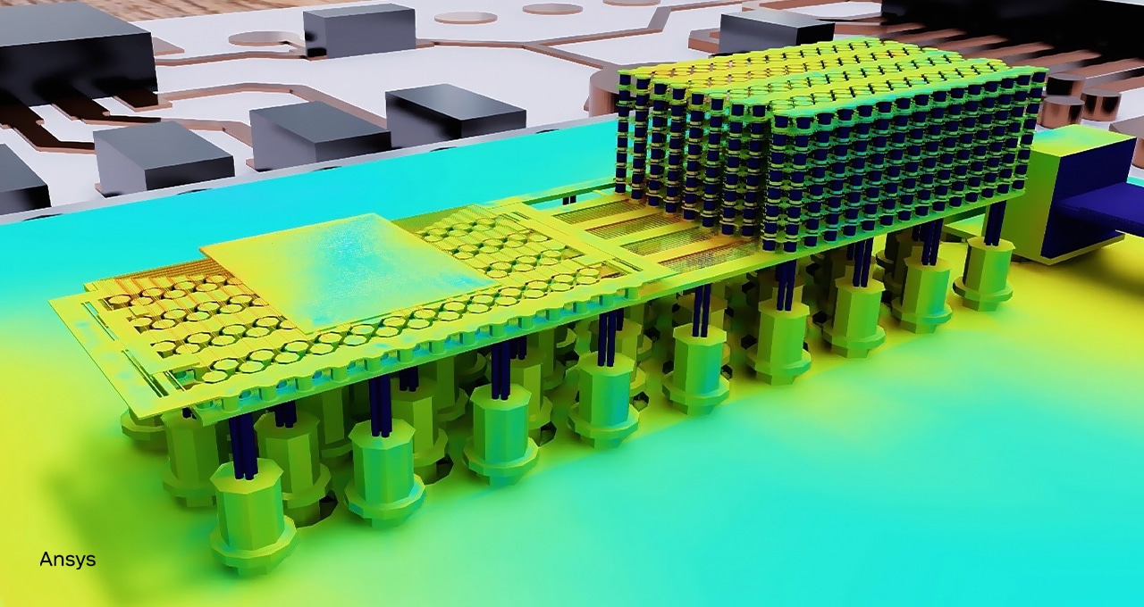
Multi-die chips, known as three-dimensional integrated circuits, or 3D-ICs, represent a revolutionary step in semiconductor design. The chips are vertically stacked to create a compact structure that boosts performance without increasing power consumption.
However, as chips become denser, they present more complex challenges in managing electromagnetic and thermal stresses. To understand and address this, advanced 3D multiphysics visualizations become essential to design and diagnostic processes.
At this week’s Design Automation Conference, a global event showcasing the latest developments in chips and systems, Ansys — a company that develops engineering simulation and 3D design software — will share how it’s using NVIDIA technology to overcome these challenges to build the next generation of semiconductor systems.
To enable 3D visualizations of simulation results for their users, Ansys uses NVIDIA Omniverse, a platform of application programming interfaces, software development kits, and services that enables developers to easily integrate Universal Scene Description (OpenUSD) and NVIDIA RTX rendering technologies into existing software tools and simulation workflows.
The platform powers visualizations of 3D-IC results from Ansys solvers so engineers can evaluate phenomena like electromagnetic fields and temperature variations to optimize chips for faster processing, increased functionality and improved reliability.
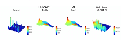
With Ansys Icepak on the NVIDIA Omniverse platform, engineers can simulate temperatures across a chip according to different power profiles and floor plans. Finding chip hot-spots can lead to better design of the chips themselves, as well as auxiliary cooling devices. However, these 3D-IC simulations are computationally intensive, limiting the number of simulations and design points users can explore.
Using NVIDIA Modulus, combined with novel techniques for handling arbitrary power patterns in the Ansys RedHawk-SC electrothermal data pipeline and model training framework, the Ansys R&D team is exploring the acceleration of simulation workflows with AI-based surrogate models. Modulus is an open-source AI framework for building, training and fine-tuning physics-ML models at scale with a simple Python interface.
With the NVIDIA Modulus Fourier neural operator (FNO) architecture, which can parameterize solutions for a distribution of partial differential equations, Ansys researchers created an AI surrogate model that efficiently predicts temperature profiles for any given power profile and a given floor plan defined by system parameters like heat transfer coefficient, thickness and material properties. This model offers near real-time results at significantly reduced computational costs, allowing Ansys users to explore a wider design space for new chips.

Following a successful proof of concept, the Ansys team will explore integration of such AI surrogate models for its next-generation RedHawk-SC platform using NVIDIA Modulus.
As more surrogate models are developed, the team will also look to enhance model generality and accuracy through in-situ fine-tuning. This will enable RedHawk-SC users to benefit from faster simulation workflows, access to a broader design space and the ability to refine models with their own data to foster innovation and safety in product development.
To see the joint demonstration of 3D-IC multiphysics visualization using NVIDIA Omniverse APIs, visit Ansys at the Design Automation Conference, running June 23-27, in San Francisco at booth 1308 or watch the presentation at the Exhibitor Forum.
